
-300x300.jpg)
-300x300.jpg)

-300x300.jpg)
-300x300h.jpg)

-300x300.jpg)
-300x300.jpg)
-300x300.jpg)
-300x300.jpg)

-300x300.jpg)
-300x300.jpg)


Semiconductor Cleanroom Guide
-1140x300w.jpg "Semiconductor Cleanroom Guide")
.jpg)
This part of our website aims to provide a guide to the issues associated with non-sterile cleanrooms used in high-tech manufacturing, particularly the semiconductor wafer fabrication operations and adjacent sectors. Each section provides an overview of the topic, as well as links to further information. It is aimed at people who are new to the semiconductor sector, or those who work in the sector in non-technical roles and want an overview of some key issues.
In section 5, the terminology is mainly related to silicon-chip based manufacturing, but the concepts also apply to any small feature technology involving photolithographic pattern generation. So, for example, it applies to wide range of semiconductor and optoelectronics manufacturing using substrates, such as: Si, GaN, GaAs, SiC, LiNbO3 etc., and some plastic electronic operations and MEMS. Terms that are commonly used in silicon microchip fabrication have been used in this guide with some explanations regarding semiconductor equipment and processes.
Contents
- 1. Cleanroom Standards
- 1.1 Cleanroom Classification Principles
- 1.2 Evolution of Cleanroom Standards
- 1.3 ISO 14644 – Cleanrooms (Series)
- 1.4 ISO 14644-1 – Airborne Particle Classification
- 1.5 ISO 14644-2 – Monitoring and Compliance
- 1.6 ISO 14644-3 – Test Methods
- 1.7 ISO 14644-4 – Cleanroom Design, Construction and Start-Up
- 1.8 ISO 14644-5 – Cleanroom Operations
- 1.9 ISO 14644-6 – Terminology and Definitions
- 1.10 ISO 14644-7 – Separative Devices, SMIF and Mini-Environments
- 1.11 ISO 14644-8 – Airborne Molecular Contamination (AMC)
- 1.12 ISO 14644-9 – Surface Particle Cleanliness
- 2. PPE Aspects of Semiconductor Manufacturing
- 2.1 Potential hazards in Semiconductor Manufacturing
- 3. Overview of why cleanrooms are needed in order to make microchips and discrete electronic components
- 3.1 The need for cleanrooms in microchip manufacturing
- 3.2 The sources of airborne particles that corrupt microchip functionality
- 3.3 Yield, Defect Density and Killer Defects
- 3.4 HEPA and ULPA Filtration
- 3.5 Laminar Airflow Design and Legacy Cleanroom Concepts
- 3.6 The impact of SMIF systems
- 3.7 Particle generation during the manufacturing processes
- 4. Other issues affecting semiconductor manufacture in cleanrooms beyond particulates
- 4.1 Inorganic Contamination
- 4.2 Organic Contamination
- 4.3 Electrostatic Discharge (ESD)
- 5. Glossary and Semiconductor Industry Insights
- 6. Useful Web Resources to Semiconductor Manufacturing
Contents
- 1. Cleanroom Standards
- 1.1 Cleanroom Classification Principles
- 1.2 Evolution of Cleanroom Standards
- 1.3 ISO 14644 – Cleanrooms (Series)
- 1.4 ISO 14644-1 – Airborne Particle Classification
- 1.5 ISO 14644-2 – Monitoring and Compliance
- 1.6 ISO 14644-3 – Test Methods
- 1.7 ISO 14644-4 – Cleanroom Design, Construction and Start-Up
- 1.8 ISO 14644-5 – Cleanroom Operations
- 1.9 ISO 14644-6 – Terminology and Definitions
- 1.10 ISO 14644-7 – Separative Devices, SMIF and Mini-Environments
- 1.11 ISO 14644-8 – Airborne Molecular Contamination (AMC)
- 1.12 ISO 14644-9 – Surface Particle Cleanliness
- 2. PPE Aspects of Semiconductor Manufacturing
- 2.1 Potential hazards in Semiconductor Manufacturing
- 3. Overview of why cleanrooms are needed in order to make microchips and discrete electronic components
- 3.1 The need for cleanrooms in microchip manufacturing
- 3.2 The sources of airborne particles that corrupt microchip functionality
- 3.3 Yield, Defect Density and Killer Defects
- 3.4 HEPA and ULPA Filtration
- 3.5 Laminar Airflow Design and Legacy Cleanroom Concepts
- 3.6 The impact of SMIF systems
- 3.7 Particle generation during the manufacturing processes
- 4. Other issues affecting semiconductor manufacture in cleanrooms beyond particulates
- 4.1 Inorganic Contamination
- 4.2 Organic Contamination
- 4.3 Electrostatic Discharge (ESD)
- 5. Glossary and Semiconductor Industry Insights
- 6. Useful Web Resources to Semiconductor Manufacturing
1. Cleanroom Standards
1.1 Cleanroom Classification Principles
Cleanrooms are classified by the cleanliness of the air within them. The classification is determined in terms of the number of particles of a particular size per volume of air. Many other aspects of these rooms may be carefully engineered and controlled, such as temperature and humidity, the electrostatic discharge characteristics of the flooring and work stations, the wavelength of the lighting in certain areas, the extraction requirements of certain equipment due to thermal loading or hazardous chemicals, but cleanroom classification is purely concerned with the cleanliness of the air in terms of particulates.
For more details, this link provides a good overview of cleanroom classifications
( https://en.wikipedia.org/wiki/Cleanroom )
1.2 Evolution of Cleanroom Standards
The boom in semiconductor technology took place in Silicon Valley California in the late 1960’s and 70’s and one of the consequences of this was that a hybrid standards system emerged whereby airborne particle counts use a combination of feet per minute, particles per cubic foot and particle sizes specified in microns. So, a class 100 cleanroom was one in which air flowed out of a HEPA (High Efficiency Particle Air) filter at 90 feet per minute and that one cubic foot of that air contained less than 100 particles greater than 0.5 microns in diameter. The American standard FED STD 209E built on this concept. Over time, new approaches were adopted to specify the allowed distributions of particles, as well as making the standards relevant to manufacturing in pharmaceuticals, semiconductors and other high-tech sectors.
FED STD 209E was cancelled in 2001 and superseded by worldwide recognised ISO standards of ISO 14644-1 and ISO 14698. Section 1.2 shows how the two different standards (FED and ISO) are related.

Historical note: EU GMP Grades A–D are used in life-science manufacturing, specifically for sterile cleanrooms, and should not be used to describe semiconductor or electronics cleanrooms. The EU GMP classifications shown in this historical table reflect the previous version of EU GMP Annex 1, which was superseded when the revised Annex 1 came into operation on 25 August 2023. FED-STD-209E is also retained for historical reference only.
1.3 ISO 14644 – Cleanrooms (Series)
ISO 14644 is a series of international standards relating to cleanrooms. It provides a common approach for defining, classifying, and managing clean environments based on measurable air cleanliness criteria.
The purpose of the standard is to provide a consistent and internationally recognised method of describing cleanroom performance. Before ISO 14644 was introduced, cleanroom requirements were often defined using regional or industry-specific standards, which made comparison between organisations and facilities difficult. ISO 14644 was developed to harmonise these approaches and allow cleanroom performance to be specified and assessed using a common methodology worldwide.
ISO 14644 is used across a range of industries, including semiconductor and microelectronics manufacturing. In this context, it provides a shared technical language for defining cleanroom performance and forms the basis on which cleanrooms are specified, tested, monitored, and referenced throughout their operational life.
1.4 ISO 14644-1 – Airborne Particle Classification
ISO 14644-1 defines the classification of cleanrooms based on the concentration of airborne particles. Classification is determined by measuring particle concentrations at specified particle sizes within a defined volume of air and comparing the results against the limits set out in the standard.
Air cleanliness is expressed using a series of ISO cleanroom classes, ranging from ISO Class 1, which represents the highest level of air cleanliness, through to ISO Class 9, which represents the least stringent classification. A lower ISO class number corresponds to a lower allowable concentration of airborne particles and therefore a cleaner environment.
Table 1 shows the maximum allowable airborne particle concentrations for ISO cleanroom classes as defined in ISO 14644-1.

The scope of ISO 14644-1 is limited specifically to airborne particulate contamination. It does not define requirements for other environmental conditions such as temperature or humidity, nor does it address process performance or product quality. The standard simply provides a consistent and measurable basis for defining and verifying air cleanliness.
For background on the historical development of cleanroom classification systems, and the transition from US Federal Standard 209E to ISO-based classification, refer to Section 1.2.
In semiconductor and microelectronics manufacturing, particle size and concentration are particularly critical because device feature sizes may be comparable to, or smaller than, many common airborne particles. As feature sizes continue to decrease, progressively smaller particles can become yield-limiting or reliability-limiting.
1.5 ISO 14644-2 – Monitoring and Compliance
ISO 14644-2 builds on the air cleanliness classification defined in ISO 14644-1 by addressing how cleanroom performance is monitored and how continued compliance with a specified ISO class is demonstrated over time. Initial classification confirms that a cleanroom meets its required air cleanliness level at a particular point in time. However, cleanroom conditions can change during operation, and ongoing monitoring is therefore required.
The standard provides principles for establishing a monitoring strategy appropriate to the cleanroom classification, its application, and the associated operational risk. This includes consideration of monitoring locations, monitoring frequency, and the conditions under which measurements should be taken in order to provide confidence that air cleanliness remains within specified limits.
ISO 14644-2 also defines circumstances in which reclassification may be required. Changes to processes, equipment, airflow patterns, or cleanroom usage can all influence airborne particle levels. The standard therefore provides a framework for determining when formal reassessment of cleanroom classification is necessary.
1.6 ISO 14644-3 – Test Methods
ISO 14644-3 defines the test methods used to evaluate cleanroom performance. These methods support both initial classification and ongoing assessment by providing standardised procedures for measuring airborne particle concentration and other parameters relevant to cleanroom qualification.
The use of defined test methods ensures that cleanroom performance can be assessed in a consistent and repeatable way, allowing results to be compared over time and between different facilities. This consistency is particularly important in semiconductor manufacturing, where small changes in environmental conditions can have a measurable impact on yield and device reliability.
By establishing recognised test approaches, ISO 14644-3 underpins the credibility of cleanroom classification and monitoring activities. It provides the technical basis for verification, audit, and periodic assessment, and supports confidence that cleanroom environments continue to perform as intended.
1.7 ISO 14644-4 – Cleanroom Design, Construction and Start-Up
ISO 14644-4 focuses on the design, construction, and initial start-up of cleanrooms, ensuring contamination control is built into a facility from the earliest stages of its lifecycle. It provides guidance on how cleanrooms may be planned and delivered to support achievement of their intended ISO classification once operational.
The standard covers key considerations such as cleanroom layout and zoning, airflow concepts, material selection, and construction detailing, all with the aim of minimising particle generation and preventing contamination ingress. It also addresses the integration of HVAC systems and building services, recognising their critical role in maintaining controlled conditions in semiconductor cleanrooms.
ISO 14644-4 also applies during the build and start-up phase, outlining clean construction practices and checks that should be completed before formal classification and performance testing take place. By following this guidance, cleanroom operators can reduce the risk of costly redesigns, delays, or failures during qualification.
1.8 ISO 14644-5 – Cleanroom Operations
ISO 14644-5 focuses on cleanroom operations and the practices required to maintain air cleanliness during routine use. While classification and monitoring define acceptable limits for airborne contamination, ISO 14644-5 addresses how day-to-day activities within the cleanroom influence contamination levels and overall performance.
The standard provides guidance on operational practices that support contamination control, including personnel behaviour, material flow, equipment usage, and housekeeping. These factors have a direct impact on airborne particle generation and distribution and often become the dominant source of contamination once a cleanroom is in operation, particularly in high-sensitivity environments.
By linking cleanroom design intent with real operational behaviour, ISO 14644-5 recognises that a cleanroom can meet its specified classification yet still fail to perform if operational discipline is not maintained. In semiconductor manufacturing, consistent adherence to defined operational practices supports stable cleanroom conditions, reduces process variation, and helps protect yield and long-term device reliability.
1.9 ISO 14644-6 – Terminology and Definitions
ISO 14644-6 provides standardised terminology, symbols, and definitions used throughout the ISO 14644 cleanroom standards series. Its purpose is to ensure that terms related to cleanroom classification, design, testing, and operation are interpreted consistently across different parts of the standard and by different stakeholders.
1.10 ISO 14644-7 – Separative Devices, SMIF and Mini-Environments
ISO 14644-7 addresses the use of separative devices to create localised clean environments within or outside a cleanroom. These devices include clean air hoods, isolators, glove boxes, and mini-environments designed to provide enhanced contamination control around specific processes or products.
In semiconductor and microelectronics manufacturing, separative devices are commonly used to achieve higher levels of cleanliness at key process steps without requiring the entire cleanroom to operate at the same ISO class. This approach allows airborne particle exposure to be reduced where it matters most, while balancing facility complexity, energy use, and operational cost.
A key application of separative devices in semiconductor manufacturing is the protection of wafers during transport and transfer between process tools. Sealed wafer handling systems reduce wafer exposure to the surrounding cleanroom environment and help limit contamination during handling and equipment interfaces.
ISO 14644-7 provides a framework for defining, classifying, and assessing these localised environments, supporting their integration into broader cleanroom contamination control strategies.
Further detail on the historical development, implementation, and impact of SMIF systems and mini-environments in semiconductor wafer fabrication is discussed in Section 3.6 .
1.11 ISO 14644-8 – Airborne Molecular Contamination (AMC)
ISO 14644-8 extends cleanroom contamination control beyond particulate matter by addressing airborne molecular contamination. Molecular contaminants, such as acids, bases, and organic compounds, can interact with sensitive surfaces and materials even when particulate cleanliness requirements are fully met.
Unlike particulate contamination, airborne molecular contamination is not detected using standard particle counting methods. As a result, a cleanroom may comply with ISO 14644-1 airborne particle classification limits while still containing molecular contaminants capable of affecting processes or materials.
In semiconductor and microelectronics manufacturing, airborne molecular contamination can influence process chemistry, surface reactions, and long-term device reliability. Sources of AMC may include construction materials, process chemicals, outgassing from equipment, and human activity within the cleanroom. ISO 14644-8 provides a framework that allows these contaminants to be assessed, specified, and controlled in a consistent manner.
By recognising molecular contamination as a distinct category, the standard supports a more complete approach to cleanroom environmental control. This is particularly important in advanced semiconductor processes, where non-particulate contamination can be yield-limiting or reliability-limiting, even in environments that meet the most stringent particulate cleanliness classifications.
1.12 ISO 14644-9 – Surface Particle Cleanliness
ISO 14644-9 addresses the classification of surface particle cleanliness, recognising that contamination on surfaces can be just as significant as airborne contamination. Particles deposited on work surfaces, tools, or components may be transferred to products during handling or processing, even when airborne particle levels are well controlled.
Surface particles are particularly problematic because they can be re-entrained into the airflow or transferred directly to products through routine handling, cleaning activities, or interaction with equipment. As a result, surface contamination can become a source of secondary airborne contamination or direct product defects if it is not properly managed.
The standard provides a framework for assessing surface cleanliness based on particle size and concentration, supporting a consistent and measurable approach to surface contamination control. This complements airborne particle classification by addressing contamination risks that arise after particles have settled and are no longer captured by airborne monitoring.
In semiconductor manufacturing, surface particle cleanliness is closely linked to handling practices, equipment design, and cleaning procedures. ISO 14644-9 therefore supports a more complete contamination control strategy when used alongside airborne cleanliness standards, helping to reduce defect risk and support stable process performance.
2. PPE Aspects of Semiconductor Manufacturing
2.1 Potential hazards in Semiconductor Manufacturing
The potential hazards incurred during the manufacture of semiconductor products are wide range. They include extremely high voltages (e.g. 200,000 volts), poisonous and/or explosive gases, strong acids, highly oxidizing substances, high pressure systems and vacuum systems, volatile solvents, radiation such as: x rays, ultraviolet, RF, and microwaves etc…
Much of the semiconductor sector is now very mature and most safety issues are well addressed by equipment manufacturers, wafer fab designers/builders and by the training given to engineers, technicians and operators. However, new employees and trainees are in a higher risk category as they may try to address a problem without fully understanding the safety issues. For example someone discovering a spillage of a highly oxidizing liquid, such as the dopant source POCl3 might reach for a handful of cellulose based non-woven wipers to wipers to contain it without realizing that they are creating a potential fire hazard (see 11.1.6 https://pubchem.ncbi.nlm.nih.gov/compound/Phosphorus-oxychloride#section=Fire-Hazards). So, if you are new to this industry take great care in dealing with unexpected abnormal events and situations and always report issues to the Emergency Response Team and/or your safety manager rather than trying to tackle them yourself.
In addition, there are the more traditional issues found in any workplace such as trip/slip hazards etc. Wafer fabs also need high levels of temperature and humidity environmental control, as part of the photolithography process, and this requires cooling towers that need to be routinely treated to protect the workforce and any nearby public from legionella.
This link takes you to a comprehensive article regarding health hazards in the semiconductor industry ( https://www.ncbi.nlm.nih.gov/pmc/articles/PMC4090871/ ) . The link provides information from the international Journal of Environmental Health 2014 Apr; 20(2):95-114
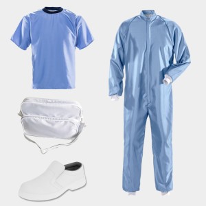
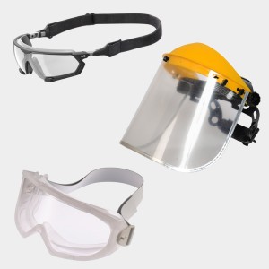
There are probably few if any firms that provide PPE covering all of the hazards mentioned above. However, Lynbond does address several of them, including protection against specific acids and solvents used in wafer fabs, as well as harmful dust inhalation. The products below have detailed specification sheets that allow appropriate choices to be made. And the Lynbond web site also allows you to search for products with specific EN numbers.
For acid aprons/coveralls click Disposable Clothing & Accessories
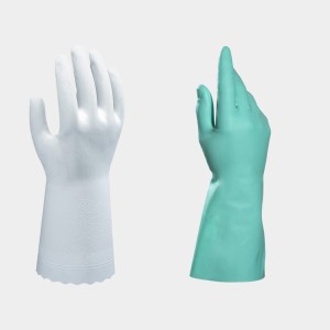
For a range of cleanroom chemical gloves click Chemical Protection Gloves
For eye protection click here
For PPE face masks click Facemasks
For a comprehensive table of PPE gloves covering acids and solvents click MAPA Gloves for the MAPPA range of products.
3. Overview of why cleanrooms are needed in order to make microchips and discrete electronic components
3.1 The need for cleanrooms in microchip manufacturing
A central element of microchip production is a printing process using a photographic technique called photolithography. Patterns are printed on to semiconducting substrates (such as silicon) many times during chip manufacture. These patterns cover the substrate in an array, looking rather like a sheet of postage stamps. Each pattern in the array has the potential to become a fully functioning microchip, but any flaw in the pattern may cause it to fail.

A silicon wafer covered in microchips
The first patterns to be printed on the substrate have features that are relatively large and each subsequent pattern has smaller and smaller features until the manufacturing stage reaches the point where tiny holes are created through which conducting layers join up the various parts of the electronic circuit. These holes are called contact holes and are typically the smallest feature on the chip. The image below shows metal tracks that join up individual parts of the electronic circuit. The small oblong features within the tracks are the contact holes. The holes are formed within insulating layers that allow the metal to make contact with the semiconductor below.

A small portion of a microchip showing the conducting metal tracks that join up components to create an integrated circuit (i.c)
The microchip is made up of layer upon layer of material, with each layer being patterned using a process called photoengraving that involves photographic and etching techniques. The details of how the layers are deposited and how they are etched is beyond the scope of this section. However, the printing process and various additional sophisticated processing allows patterns to be created in each of the deposited layers. The image below shows an idealised three-dimensional schematic of part of a microchip. It gives an idea of how patterned layers are built up to create a complex tangle of various materials that forms the electronic circuit.


A 3D schematic illustrating the complex layering of a microchip and an actual cross section
In many cases, the components within a microchip operate at low voltage and with tiny electrical currents. What this meant in the early days of the industry was that the patterns being printed were larger than they needed to be. As a result, there was a technological race to achieve improved printing capabilities. At the end of the 1970’s the smallest features (usually the contact holes and the metal tracks that joined them) were 5 microns wide. By 2020 features 500 times smaller were possible, with lines as narrow as 10 nm being printed in the leading-edge wafer fabs.

The graph shows the ability to create features of a particular size (the red shows the wavelength of light used in the processing)
Finally, we get to answer the question of why microchips are made in cleanrooms. The answer is that airborne particles landing on the substrates (e.g. silicon wafers) during microchip manufacturing caused defects in the printing process that meant that the microchips failed to operate properly. The ratio of the number of chips on a silicon wafer that work compared to the total number on the wafer is called the die yield. And sometimes, in the early days, the yield could be less than 10%. In other words, 90% of the chips on a completed silicon wafer could be scrap.

Every microchip on this wafer was tested against a specification, those with black dots on them failed and are scrap.
3.2 The sources of airborne particles that corrupt microchip functionality
The corruption of the printed patterns on a semiconductor wafer could be due to many causes. Some of the causes are due to process/equipment limitations that might produce a non-random scatter of defects. Other defects, such as airborne particles, are of a more random nature. Imagine a silicon wafer that has 1000 completed microchip patterns printed onto it and has accumulated 100 randomly positioned defects due to airborne particles. In this case at least 900 of the chips will not be affected by the 100 random defects, so the yield will be over 90%. Now consider the case where the microchips were much larger, for example if only 10 microchips were printed onto the silicon wafer, then 100 random defects would mean that probably all those chips would fail. The point is that airborne particles can have a dramatic impact on the levels of scrap produced during microchip manufacturing.
In fact, as chip sizes increase and the feature size on the chips decrease then scrap due to airborne particles rapidly increases. So, the aim of cleanrooms is to control airborne particles in order to reduce the levels of defects that cause microchips to fail. Note also that not all defects cause the chips to fail, those that do are called killer defects. Some defects do not immediately cause failure in the chip but might reduce its reliability. There are also some defects that are visually undesirable, but which are benign.
3.3 Yield, Defect Density and Killer Defects
Airborne particles landing on the semiconductor wafer might corrupt the chip pattern, or they might interfere with the deposited layer causing a void, or, as in the image below they might create a potential electrical short circuit between two conducting metal tracks etc...

The nature of the particles causing problems can be wide range and the image below shows the types of airborne particles that cleanrooms try to eliminate.

Particles that can be airborne poster from https://www.visualcapitalist.com/wp-content/uploads/2020/10/relativesizeofparticles.html
The two images above illustrate some of the challenges of microchip production. The first one shows how a particle of about 25 microns in length can impact a microchip with features of about 5 microns. The second image shows that even a grain of pollen would be problematic in the 1970’s where features on microchips were as small as 5 microns across. At that time, microchips were being manufactured with minimum feature size of 5 microns and so particles of 0.5 microns landing on the silicon wafer could have a 10% impact on the width of a feature. During this era cleanrooms used for semiconductor integrated circuit production were being constructed aimed at removing particles above 0.5 microns from the manufacturing area. Back then, microchip patterns could be designed to work properly even if some 0.5-micron particles landed on them.
In the 1970’s most semiconductor (wafer fab) cleanrooms were classified as Class 100. This meant that an unmanned cleanroom would contain air with less than 100 particles greater than 0.5 microns per cubic foot of air (Section 2 of this guide provides further details of cleanroom classifications).
Unmanned cleanrooms met their specifications, but when people entered them they, and their clothing, were sources of unwanted airborne particles and contaminants. Table 1 shows the sources of particles/contaminants from people and the way to minimize their impact.
Table 1
Possible particle/contaminant source | Mitigation strategy | Comments |
Dust and other particles shed by clothing | Wearing of a coverall made from a specialised polyester material. | Coveralls are widely used in
cleanrooms. For static sensitive products conducting fibers can be woven into
the fabric of coveralls and heal grounders worn. In general, cleanroom
flooring is antistatic and requires special cleaning to maintain this
property. |
Hair, dandruff and flakes of skin | Wearing of a balaclava style hood made from a specialized polyester
material. | For practical purposes some hoods have
coarse mesh ear covers to aid hearing. |
Facial hair, respiratory droplets and tobacco smoke particles. | Wearing a face mask or face veil. | These face masks and face veils are not PPE; they are to protect the
wafers from personnel. |
Make-up | Cleanroom personnel are often banned from wearing make-up. | A discipline issue that requires clear communication and regular reinforcing. |
Jewelry | Cleanroom personnel are often banned from wearing jewelry. | The consequences of a gold earring being lost and contaminating a microchip
production line can be devastating. |
Hands shedding skin particles and perspiration. | Barrier gloves are made from vinyl, nitrile rubber or latex rubber. | As with other items in this table, gloves are to protect the wafers
from people. Cleanroom gloves come in various grades from power free through
to low particle gloves specified for particular cleanroom classes. Vinyl
gloves are generally the cheapest. Nitrile
gloves are higher quality and can have better ESD performance. Latex gloves are robust and very elastic, but they
are associated with a skin allergy affecting between 4 and 17% of workers
(see NHS link below this table). Some chemical elements pose a major concern for silicon microchip
manufacturing, one of them is sodium (Na) which is found in perspiration as a
constituent of common salt (sodium chloride - NaCl). Barrier gloves help to
reduce this contaminant from reaching the semiconductor substrates |
Shoes | Normal shoes bring dirt into the cleanroom on the sole and the upper. | The lowest and cheapest approach is to use overshoes. They help
contain the dirt on the shoe, but thin cheap overshoes wear through into
holes. Holes allow contaminants through and the material that disappeared to
create the hole becomes dust that itself contaminates the cleanroom. Thicker quality shoe covers help to reduce these
problems. A higher level of protection is to use overboots,
sometimes both shoe covers and overboots are worn. Cleanroom
shoes are also an option that offers greater comfort and they may be
less of a trip hazard. |
Link to NHS web site with information regarding latex skin allergies.
(https://www.nhshealthatwork.co.uk/images/library/files/Clinical%20excellence/Latex_allergy_full_guidelines.pdf)
3.4 HEPA and ULPA Filtration
High Efficiency Particulate Air (HEPA) and Ultra-Low Penetration Air (ULPA) filtration are the primary methods used to control airborne particulate contamination in cleanrooms. These filters form part of the air handling and recirculation systems, removing particles from the air before it is reintroduced into the cleanroom environment.
A typical 1970’s wafer fab cleanroom was a room fitted with HEPA filter modules above all workstations. Air was pumped into the room through pre-filters and then through the HEPA filters. Air flowed through the HEPA filters at about 90 feet per minute. The air is intended to flow in a laminar fashion (not turbulent, or chaotic). For processing reasons, the temperature and humidity of the air has to be controlled and for economic reasons it is recirculated with approximately 10% fresh air added at each cycle.
See diagram below for a basic cleanroom configuration.

Here is a class 100 cleanroom. HEPA filters, housed in a row of blue Vertical Laminar Flow units, supply filtered air above the work areas at 90 ft/min.
HEPA filters are designed to remove at least 99.97% of airborne particles with a diameter of 0.3 µm, which is considered the most penetrating particle size. For both larger and smaller particles, actual filtration efficiency is typically higher. This level of performance represents a practical balance between particle removal efficiency, airflow resistance, energy consumption, and maintenance requirements, making HEPA filtration suitable for a wide range of cleanroom classes.
ULPA filters provide a higher level of filtration than HEPA filters, removing at least 99.999% of particles down to approximately 0.12 µm. This increased performance is achieved through denser filter media, which results in greater resistance to airflow and higher energy demand. For this reason, ULPA filtration is typically reserved for environments where extremely low airborne particle concentrations are required.
In semiconductor and microelectronics manufacturing, the choice between HEPA and ULPA filtration is driven by the required cleanroom classification, process sensitivity, and overall system design considerations, including airflow architecture and energy use. HEPA filtration is sufficient for many applications, while ULPA filtration is used where even very low levels of particulate contamination can impact yield or long-term device reliability.
HEPA Vs ULPA Filters In Cleanrooms - CSI Testing
ULPA vs HEPA Fan Filter Units: A Cleanroom Filtration Guide
3.5 Laminar Airflow Design and Legacy Cleanroom Concepts
Laminar airflow is a fundamental cleanroom design principle used to control the movement of airborne particles and minimise contamination risk. In a laminar airflow system, filtered air moves in a uniform, unidirectional flow, typically from the ceiling towards the floor, carrying particles away from contamination-sensitive process areas.

Figure 2 illustrates a typical vertical laminar airflow cleanroom configuration, showing HEPA filter modules supplying air from the ceiling and the return air path at floor level.
In semiconductor and microelectronics cleanrooms, laminar airflow has traditionally been supplied through ceiling-mounted HEPA or ULPA filters. The air flows vertically downward in parallel streamlines, reducing turbulence that could cause particles to remain suspended or be redistributed onto sensitive surfaces such as silicon wafers or process equipment.
The effectiveness of laminar airflow depends on maintaining a consistent airflow velocity across the cleanroom. If airflow is too slow, particles may settle or recirculate. If airflow is too fast, turbulence may be introduced, increasing the risk of particle re-entrainment. Airflow velocities are therefore carefully specified during cleanroom design to balance particle removal with energy efficiency and process stability.
Obstructions within the airflow path, such as equipment, workstations, or personnel, can disrupt laminar flow and create localised turbulence or eddies. Cleanroom layouts are designed to minimise these disturbances by controlling equipment placement, work height, and operator positioning relative to the airflow direction.
Laminar airflow systems are particularly important in higher-grade cleanrooms, where airborne particle limits are more stringent. By continuously sweeping particles away from critical process areas, laminar airflow supports stable environmental conditions and helps maintain consistent cleanroom performance over time.
3.6 The impact of SMIF systems
The cleanroom wafer fabs of the 1970’s made silicon chips in batches of 25 or 50 silicon wafers. The silicon wafers were carried around the production area in jigs called cassettes that were put into boxes with a set of process instructions attached to each box.


Silicon wafers in cassettes A wafer cassette in a cassette box Wafer held by a vacuum wand
As each step of the process was completed, data was added to the process instruction sheet and information was also entered into a computer system that kept track of each box.
Wafers were removed from the boxes inside the cleanroom and then loaded into high-tech equipment for processing.
Sometimes the equipment accepted the cassettes and removed the wafers automatically.

Cassette based loading/unloading of a sputtering machine
Sometimes the silicon wafers were transferred from a cassette using tweezers

Silicon wafers manually loaded onto a quartz furnace boat using tweezers
So, in the 1970’s and 1980’s there was a lot of manual loading of semiconductor substrates into and out of processing equipment. Silicon wafers were exposed to the environment of the cleanroom, and they were vulnerable to airborne contamination during these times. The techniques for handling wafers also put them in jeopardy of being scratched or damaged in other ways. As the industry matured, its wafers got bigger and the features on them got smaller and new ways of reducing particulate contamination and mishandling were being developed in the direction of far greater automation of substrate handling. The aim was to keep the substrates safe in their own mini environmental box throughout their manufacturing journey, except when they were undergoing a processing stage. To do this a special wafer carrier was developed called the Standard Mechanical Interface (SMIF https://en.wikipedia.org/wiki/SMIF_(interface))
And, importantly, equipment manufacturers began designing their equipment to be SMIF compatible.

A SMIF wafer carrier.

An Eaton Nova Axcelis implanter with SMIF capability
The use of SMIF meant that wafers could be protected from particles without needing the whole production area to be super clean, so leading edge chip makers could save money on their cleanrooms by having selected areas very clean, but not the whole area. Cleanroom clothing and cleanroom procedures and disciplines were maintained, but large ballroom environments of super clean air were no longer necessary.
Leading edge chip makers are mainly located in South East Asia and they process 300 mm diameter silicon wafers and print features that are less than 10nm wide. There are no semiconductor manufacturers like this in the UK. Instead, there are many specialist wafer fabs that create value through their technical expertise in niche areas. They create leading edge products in: silicon, gallium arsenide, silicon carbide, lithium niobate and other exotic materials, as well as pushing the boundaries of ultralow cost products in the area of plastic electronics. These wafer fabs utilize legacy silicon processing equipment in traditional cleanrooms that are kept as clean as possible.
In the context of the global semiconductor sector, the UK wafer fabs are niche operations. They modify and develop unique equipment and processes that create synergies leading to wealth creation. They tend to swim in the shallows and don’t really compete with the leading silicon-based firms. They rely on cost effective legacy equipment, expert ‘know how’ and leading-edge intellectual property. It may be that SMIF eventually ends up in more UK fabs, but this will only happen if it offers economic benefits. Time will tell.
3.7 Particle generation during the manufacturing processes
This is an area that leading edge silicon fabs have been exploring for the past few years. As wafer size increased and feature size decreased this sector of the industry discovered that despite keeping wafers in very clean environments throughout their processing by using SMIF technology, robotics and automation, they still had yield losses, and these were not due to traditional airborne particles. Instead, the defects were coming from the processes themselves.
Leading edge silicon chip makers have all but beaten airborne particle contamination and now look at the equipment and chemicals for the sources of defects. So, processes, parameters, maintenance and preventative maintenance procedures and cleanliness of chemicals (gasses and liquids) have all come under greater scrutiny. Along with this the metrology and analytical equipment sector has been challenged to provide new tools and techniques. It seems possible that these new insights into semiconductor processing may be a new source of competitive advantage for the UK high-tech manufacturing sector, but this is, as yet, unclear.
4. Other issues affecting semiconductor manufacture in cleanrooms beyond particulates
Whilst a cleanroom, and SMIF technology, reduces the impact of particulates on microchip production it is not the only challenge. There are other forms of contamination that can cause microchips to fail to work properly and this section touches on some of them that arise within a wafer fab.
4.1 Inorganic Contamination
The silicon manufacturer, SEH, has a web site shows that the silicon wafers that it produces for chip makers is 99.999999999% pure silicon, also called eleven nines pure ( see this link https://www.shinetsu.co.jp/en/products/electronics-materials/silicon-wafers/ ). The reason that the silicon needs to be so pure is that contaminants within the silicon reduce the performance of the microchips. This fact has been known for decades. Along ago as 1969, Arpad A Berg and G.H. Schneer published a paper called ‘The Effect of Ionic Contaminants on Silicon Transistor Stability ( see this link for more details https://ieeexplore.ieee.org/abstract/document/5216974/authors#authors ). Berg and Schneer’s research demonstrated a need for ultrapure silicon and manufacturers like SEH, Wacker, Monsanto etc. rose to the challenge. They have been creating purer and purer silicon ever since. Unfortunately, whilst the silicon begins pure it collects contaminants during its journey through wafer fab. Many such contaminants are added to the silicon wafer during its conversion from a pure silicon wafer to a wafer that is covered in functional electronic devices. There are many sources of contamination, but for this guide only those originating from human bodies are relevant. In 2001, Makato Takiyama published an interesting paper. In it he stated that contaminants such as Al, Cr, Cu, Fe, Ni and Zn originated from the processing equipment whilst Ca, K and Na contaminants from the human body (see this link for more details https://www.nipponsteel.com/en/tech/report/nsc/pdf/8314.pdf ). So, clearly, the transfer of Calcium (Ca) Potassium (K) and Sodium (Na) from wafer fab personnel has to be minimised. This can be achieved by covering wafer fab personnel with appropriate clothing and making sure that the clothing is not a source of Ca, K or Na.
This article (see link https://www.ncbi.nlm.nih.gov/pmc/articles/PMC6776299/ ) in the National Library of Medicine gives insights into where the Ca, K and Na contamination is coming from. In the article’s introduction it states”
“It has been well documented that eccrine sweat produced for evaporative cooling in humans contains water, electrolytes, lactate, ammonia and urea. The electrolyte predominantly consists of Na+ and Cl - and to a lesser extent K+, Mg+ and Ca+.”
Also, the archives of Oral Biology volume 48, issue 5,May 2003 pages 337 to 344 ( see this link https://www.sciencedirect.com/journal/archives-of-oral-biology ) show that saliva also contains Na+ , K+ and Ca+
So, whilst cleanroom apparel of: Hood + Facemask/Veil + Coverall +Gloves+ Overboots all reduce the transfer of particles it is also necessary that the gloves and facemask do not transfer saliva or sweat to wafers or any other items of wafer fab equipment. Lynbond provides a range of clothing with low levels of Na, K, Ca and Mg which can be found in the links below.
Cleanroom Hoods / Caps
Facemasks
Cleanroom Clothing
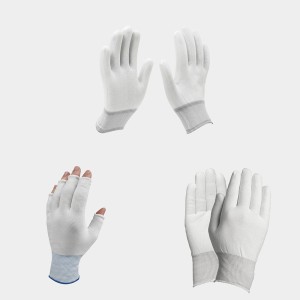
Gloves
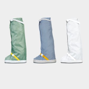
Cleanroom Boots
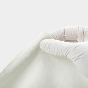
Furthermore, people bring wipers into the wafer fab to clean equipment or wipe up spills, and it is essential that these items too have low levels of Na, K and Ca. The link below shows a range of cleanroom wipers with low levels of alkali metals Na, K , Ca and Mg.
Cleanroom Wipers
4.2 Organic Contamination
Historically, most issues regarding organic contamination fell into two areas airborne or waterborne.
Airborne organic particles such as flakes of skin, grains of pollen, respiratory droplets and other organic particles are mainly captured by the HEPA filters as discussed in the section on cleanrooms. Organic particles that are not captured by the filters get into the wafer fab and are dealt with various surface cleaning processes such as acid or plasma cleaning processes that recur throughout the creation of a microchip.
Another source of organic contamination can be found in the deionized (DI) water that is used in many cleaning operations. This is called the Total Organic Carbon (TOC) level of the water. The starting point for DI water can be from different sources, such as confined or unconfined aquifers (as shown in the figure below).

Different sources of water have different chemical signatures, with the organic carbon load originating from natural organic matter, organic pollutants, pesticides etc... TOC levels can vary and could be well over 10ppm in the water directly from an aquifer.
To cope with variations presented by a specific source of water, the DI system of a particular wafer fab may have a water purification process tuned to the source of the water. After purification the TOC level in the DI water used in a wafer fab is likely to be in the range 0.1ppd to10 ppb. For more details here is a link to a reputable DI water specialist https://www.elgalabwater.com/blog/total-organic-carbon-toc.
In addition to the carbon found in aquifer water, there is a possibility of bacterial populations growing in the DI pipework within the wafer fab. These bacteria could compromise the processing and depress yields. As stated in a report by the American Society for Microbiology ‘…piping, membranes, tanks, and other surfaces within the UPW system provide favourable places for bacterial adhesion and cell growth’. See this link for more details ( https://www.ncbi.nlm.nih.gov/pmc/articles/PMC123900/ )
Since the origins of the DI water is one source of contamination, the locations of some wafer fabs have been built with the source of the DI water in mind. For example, the Matsushita wafer fab in Arai in Japan, was located there to benefit from water melting from the top of nearby mountains and being particularly clean.
4.3 Electrostatic Discharge (ESD)
Many electronic devices are vulnerable to being damaged by an electrostatic discharge. Such vulnerability can be present during their manufacture and when being assembled into final products. The ESD Association (see link https://www.esda.org/ ) sets global standards and provides training and certification regarding this issue.
Below are products that Lynbond provides to mitigate ESD issues. Click on the links for their full specifications.
ESD cleanroom hood
ESD cleanroom clothing
ESD overshoes
ESD heel grounder
ESD wrist strap
5. Glossary and Semiconductor Industry Insights
Aligner – see Photolithographic aligner.
Barrier glove – a glove that is intended for use in a wafer fab cleanroom. Its aim is to reduce the chance of human perspiration from being transferred onto electronic substrates or other equipment. The main concern is to stop ions of Na, K, Ca or Mg from contaminating silicon wafers since this can cause excess leakage currents to be present in the finished product. One consequence of high leakage can be that the product fails to meet its specifications, or that it presents a reliability issue. In simple terms, one effect of high leakage currents can be a shortened battery life in mobile devices, like phones, tablets etc... Barrier gloves are typically thin non-handed 12” long and made from Vinyl, Nitrile or Latex
Contact aligner – this is a photolithography tool that shines light through an image on a photomask and onto a wafer. The wafer, which is covered in photoresist, is positioned under the photomask and the relative position of the wafer and photomask can be adjusted. The adjustment allows the photomask to be accurately positioned with regard to a family of patterns already on the wafer. When the alignment is correct the wafer and photomask are bought into contact with each other. Then light is shone through the photomask to expose the photoresist on the wafer. Bringing the wafer and mask into contact gives sharp edges to the features and helps to achieve the minimum feature size. This type of equipment had the disadvantage that the mask became increasingly damaged as more and more wafers were processed. Early photomasks were made from cheap glass soda glass and the patterns on them were relatively soft photographic emulsion that was easily damaged. So, these types of photomasks were discarded after 25 or 50 wafers had been processed with them.
Diffusion Furnace – Diffusion furnaces are used to deposit dopant atoms onto the surface of substrates and then to facilitate the redistribution of the dopant so that it diffuses beneath the surface of the wafer. They are also used to redistribute dopant atoms that have been implanted in a wafers surface and to anneal and activate implanted layers. Diffusion furnaces are also used to grow oxides on wafer surfaces.
Modified diffusion furnaces that operate at low pressures can also deposit a variety of layers (such as oxides or nitrides) onto the surface of wafers using Low Pressure Chemical Vapour Deposition (LPCVD) techniques.
Diffusion furnaces may be horizontal or vertical and can be single furnaces or configured as a group (e.g. a four-stack horizontal furnace). Horizontal furnaces were used in silicon processing for wafers up to 6” in dia. Larger wafers are generally processed in vertical furnaces.


Thermco horizontal furnace Thermco vertical furnace
Discrete or Discrete device – is an electronic device such as a transistor, diode, thyristor, semiconductor controlled rectifier (SCR) etc... Whilst a silicon substrate might be covered in discrete devices, they are individual entities and are not connected together to form an integrated circuit. When the silicon wafer has completed its process journey through the wafer fab stage it will be sawn up so that each discrete device (such as a single transistor) can be separately packaged .


Some packaged transistors, A single transistor before it is packaged
which are discrete devices
Electrostatic Discharge abbreviated to ESD – A discharge of static electricity following the buildup of charge, often due to materials rubbing together. ESD can cause microchips to fail and increase the levels of scrap. There are many ways to mitigate this issue. A good starting point to understand ESD issues is the ESD Association (see link https://www.esda.org/ ) .
Ellipsometer – A measurement instrument capable of measuring refractive index and/or thickness of a thin film.
Epitaxy reactor – This equipment deposits a layer of silicon on top of a silicon wafer in a manner that maintains the single crystal nature of the wafer. Dopant atoms are incorporated into the deposited layer during the deposition process, enabling a uniform level of the dopant atoms to be created in the newly deposited layer. Epitaxy layers can be deposited onto substrates other than silicon. Early reactors processed batches of wafers that had to be manually loaded and unloaded. More recent models can deposit epi onto single wafers utilizing automated loading and unloading.
Early epitaxy reactors incorporated atmospheric deposition conditions which resulted in pattern shift and associated alignment issues. Later equipment allowed for low pressure deposition where zero pattern shift can be achieved.


Thermco epitaxy reactor manual loading Gemini epitaxy reactor Manual loading

Applied Materials Centura single wafer epi with automated cassette to cassette SMIF loading
Exhaust Gas Scrubber – most processes do not consume all of the gasses/vapours within the reaction chamber and so they and any byproducts from the process have to be dealt with and made safe. Depending upon the specific chemicals, one approach is to pass the effluent biproducts through a chemical scrubber. More details of how a scrubber works can be found at this link https://en.wikipedia.org/wiki/Scrubber.


A schematic of one type of chemical scrubber What a typical scrubber looks like
Face mask - In the context of a wafer fab, the basic face masks that are required to be donned by anyone entering the cleanroom are primarily spit guards to stop respiratory droplets from contaminating the wafers. The main concern is to stop ions of Na, K, Ca or Mg (that are found in saliva) from contaminating silicon wafers since this can cause excess leakage currents to be present in the finished product, the consequences of this can be that the product fails its specification, or that there is a reliability issue. In simple terms, one effect of high leakage currents can be a shortened battery life in mobile devices like phones etc...
Specialist PPE face masks and respirators are specified for use following risk analyses of hazards.
Film thickness measurement - Many different films exist in a microchip and even more exist during the manufacture of the chip. See the following for instruments that measure a variety of parameters on a variety of film types: FTIR Spectrometer, ellipsometer and Nanospec.
Flat finder - Semiconductor substrates are predominantly cut from a single crystal ingot and knowing the orientation can be important, so a flat or notch is incorporated in the wafer (historically, bipolar devices were made on <111> silicon whilst MOS devices were formed on <100> silicon). Many machines automatically position the wafer in the correct crystallographic position, but early batch processing equipment sometimes required the wafers to be aligned using simple gadgets as shown below.


Manual flat finder Automated notch finder
Fourier Transform Infrared Spectrometer (FTIR) – A measurement instrument capable of measuring the thickness of epitaxial layers.


AVANT ES200 automated FTIR epi thickness instrument Nicolet FTIR benchtop epi instrument
Four-point probe – This equipment measures the surface resistivity of the wafer. It places four equally spaced needle like electrical probes onto the wafer and then supplies a known current through the two outer ones whilst measuring the voltage on the two inner ones. It measures the sheet resistivity of the wafer in ohms per square. It is often used as a proxy measure for the quantity and depth profile of a dopant layer that has been achieved during processes such as diffusion ion implantation. It can also be used on metal deposition processes. Four-point probe measurements are used as a process control/SPC measurement. However, many diffusion profiles could achieve an ‘in spec’ result. So, it shows when a process is definitely out of specification, rather than proving that it is correct (i.e. an in spec’ reading is a necessary but not sufficient condition for the wafer to be considered good).


A Veeco four point probe machine A Jandel four point probe head
Gas cabinet – Gas cabinets are metal cabinets where pressurized gas bottles are kept. Flammable and poisonous gases are kept in extracted cabinets that have detector /alarm systems added to them.


Schematic of basic gas cabinet. Gas cabinet showing controls & gauges
HEPA filter – High Efficiency Particle Air Filter These filters remove particles from the air moving through them. The filter allows air to pass through it and particles that are smallest pore size are physically sieved out of the air.
HMDS – HexaMethyDiSilazane is an adhesion promoter used in photolithography. See this link for details of some surface preparation techniques: https://www.microchemicals.com/technical_information/substrate_cleaning_adhesion_photoresist.pdf
Horizontal Laminar Flow unit or module - is a box with an air inlet and an outlet for the air through a HEPA filter. The HEPA filter covers almost one complete side of the box. These units are often built into the rear side of a standalone workstation within a controlled environment that does not have 100% VLF coverage. For example, in a maintenance area where a clean space is needed for inspecting/disassembling/reassembling sensitive components.

Horizontal laminar flow workstation with air drawn in from below and then blown out through a HEPA filter to maintain a clean work area
Integrated Circuit or an ic – is an electronic circuit comprising of many components that have been created on a single piece of semiconducting material or other type of substrate.
Ion Implanter – a particle accelerator that ‘sprays’ the surface of a wafer with ions of a specific element. The atoms penetrate the surface of the wafer with a predictable depth and distribution.
LPCVD - Low Pressure Chemical Vapour Deposition
Mass flow controller (MFC) – Mass flow controllers are found within many processing tools; they accurately control the mass of gas being introduced into a process chamber.
Microchip – a popular name for an integrated circuit.
Nanospec – This is an instrument that measures the thickness of films whose refractive index is already known. It is often used to measure silicon dioxide films and photoresist films and sometimes thermal nitride films if the refractive index is well controlled.

Nanometrics Nanospec AFT film thickness measurement tool
Photomask –Microchips are made up from many patterned layers of various materials. The patterns are formed by a process called photoengraving that involves turning the silicon wafer into a photographic plate by coating it in a photosensitive layer called photo resist and then exposing an array of patterns onto the wafer. The array of patterns is first created on a glass (or quartz) plate called a photomask. The photomask is positioned above the wafer and light is shone through the mask to create a duplicate image in the photoresist on the wafer surface. The wafer is then developed to remove unexposed photoresist, heated to harden the exposed photoresist and then etched. The exposed photoresist etches much slower than the underlying layer and therefore protects the layer beneath it from the etchant. So, after etching, when the resist is finally removed from the wafer it reveals a pattern in the layer below.
(Go to the photoresist section for a schematic of the basic photolithographic process)

A photomask in an open mask box (note: ungloved hands would never be allowed in a wafer fab)
Photoresist (also just called resist) – A photosensitive liquid that is applied to the surface of wafers to turn them into photographic plates. A drop of the liquid is dispensed onto the centre of a wafer, and the wafer is then spun to disperse the liquid and creates a uniform coating across the surface of the wafer. It is then heated at a low temperature to drive off the solvent. An image is then projected onto the surface, and the wafer is developed to remove certain areas of the resist.
Two basic types of resists are available, negative resist where regions exposed to light are retained on the wafer during development, and positive resist where exposed regions are removed during development. After exposure, the wafers are heated again to harden the resist. Both kinds of resist protect the areas beneath them from being etched by subsequent etch processing. Finally, after the wafers have been etched, the resist is removed creating a wafer with an etched pattern upon it.
Here is a link with more details https://www.sciencedirect.com/topics/engineering/photoresist

Pellicle – A pellicle is a thin, taught, transparent skin that is applied to stepper reticles. It is positioned a few mm above the patterned side of the reticle by being attached to a raised frame. Its purpose is to stop particles landing directly on the reticle pattern and corrupting it. It works because particles falling onto the pellicle are not in the focal plane of the reticle/photomask when the pattern is being exposed and therefore the particles will be out of focus and not be printed. Here is link providing more details
https://spie.org/publications/spie-publication-resources/optipedia-free-optics-information/pm146_78_pellicles#_=_

A pellicle, showing the frame supporting the thin transparent stretched skin that is attached to the reticle.
Photolithographic aligner (or just aligner) – Four types of aligner are discussed in this glossary. The oldest type is a Contact aligner. The next oldest is a Proximity aligner, the next is the Projection aligner and the most recent is a Stepper. As a rule of thumb, Contact were used with silicon wafer up to 4” in dia. Proximity and Projection were used with silicon wafers between 4” and 6” and Steppers were used for silicon wafers of 4” and above. Technologies using other substrate types and hybrid technologies (such as MEMS) may use any of the four types depending upon their specific needs.
Projection aligner - this is a photolithography tool that projects light through an image held on a photomask onto a wafer. The wafer, that is covered in photoresist, is positioned some distance from the photomask and the relative position of the wafer and photomask adjusted. The adjustment allows the photomask to be accurately positioned with regard to a family of patterns already on the wafer. Unlike its predecessor (the proximity aligner) the photomask and wafer are physically some distance apart in the machine and an even larger optical distance due to the use of mirrors. The projection aligner was revolutionary and optically very sophisticated in its day, and details of its development and comments on earlier aligners can be found using this link https://en.wikipedia.org/wiki/Micralign
Proximity aligner - this is a photolithography tool that projects light through an image held on a photomask onto a wafer. The wafer, that is covered in photo resist, is positioned under the photomask and the relative position of the wafer and photomask adjusted. The adjustment allows the photomask to be accurately positioned with regard to a family of patterns already on the wafer. Unlike its predecessor (the contact aligner) the photomask and wafer are positioned so that there is a small uniform gap between them. This gap prevents damage to the mask, which gives it a long life and allows high quality photomasks to be adopted.
The higher quality photomasks are made from materials that have similar expansion coefficients to silicon, which reduces the phenomena of run-in/run-out. Such masks also have patterns on them that are made of chrome (rather than photographic emulsion) which also extends the life of the mask as it can be cleaned using quite aggressive cleaning techniques.
Reticle – A reticle is a particular kind of photomask that is used by a stepper. The reticle may contain a single pattern of one layer of a single microchip (as shown below) or for smaller microchips it may contain a small array of patterns. When used in production the array is most often all of the same microchip, but during the development of a chip several variations can be included within the array. Also, several Universities may include various patterns on a single reticle in order to reduce costs of production.

A reticle for a stepper (Note: a reticle would never be handled as shown until it has become obsolete or damaged)
A schematic of one type of chemical scrubber What a typical scrubber looks like
Quartz ware – Many chemical reaction chambers that are required to reach temperatures up to 1250 deg C are made from very high purity quartz. They include furnace tubes, wafer carriers/boats, gas injectors, epitaxy bell jars, gas baffles, etc...


Examples of quartz ware used in semiconductor processing.
Statistical Process Control (SPC) – Leading edge microchip manufacturing has always used processes that were/are at the limit of their capability envelope. In the early days, processes, environmental control and measurement limitations resulted in significant amount of scrap being produced. The whole industry was in a dynamic state with improved equipment and processes regularly being adopted by the sector. Two important approaches that were aimed at reducing scrap and lowering costs were design for manufacturability (DFM) and statistical process control (SPC).
DFM involves designing and engineering a product to minimize manufacturing costs and it occurs outside the wafer fab at the design and development stages. So, it is not covered here, but this link provides some more details https://en.wikipedia.org/wiki/Design_for_manufacturability
SPC is an approach to process control that aims to identify the causes in process variations by analyzing the measurements taken at each stage of manufacture. Two types of variation are identified. One of the causes is called common and refers to variation that exhibits a gaussian distribution (one that produces a bell-shaped curve when plotted as a histogram). This type of variation shows the limitations of the process, rather than it being out of control. If this type of variation is unacceptable (if it generates scrap) then fundamental changes to the processing system are needed, such as replacing equipment with more capable machines. The second cause of variation is called special, in this case a specific phenomena is involved that should be identifiable and then it can be addressed to bring the process under control. For example, if a newly cleaned item of equipment gives a low result and each subsequent process run increases until it needs cleaning again then that would be considered out of control and one solution would be to clean the equipment after every process run. This example was quite common in the early days of chip production. Systems would be set up to run at the bottom end of the specification after cleaning and then cleaned again after many runs just before measurements reached the top end of the specification. Statistically the process was out of control, but the outcomes of many runs were within the specification limits. Such an approach could have unintended consequence in not being the cheapest way to manufacture the chips.
For more details regarding SPC follow this link https://en.wikipedia.org/wiki/Statistical_process_control
An alternative method of reducing scrap, creating more consistent microchips and achieving the best overall product cost is the Taguchi approach (see this link https://en.wikipedia.org/wiki/Taguchi_methods ) . Basically, Taguchi advocates reducing process variation and achieving results for each process run that are always on target.
Surfscan - A Surfscan is a tool for identifying the source of defects. It identifies defects on patterned wafers. Pristine wafers can be run through the machine to identify their background level of defects/particles and then the wafer can be run through a process to see how many defects are added. Wafers might be processed through a full process. Or they might just be run through the system to see how many defects the handling stages add. Historically, witness wafers were left at positions in the clean room to see how many particular defects were added. In a SMIF environment this may be less helpful than checking the SMIF handling system and associated wafer handling within the process equipment itself.

Surfscan SP7 defect identification tool.
Susceptor – In the context of semiconductor manufacturing, within a wafer fabrication area, a susceptor is a component that holds the substrate during processing. The susceptor may be made of various materials, for example the core may be graphite with a coating of silicon carbide. The images below show a variety of susceptors with circular recesses where the substrate wafers are to be located.

Silicon wafer, also simply called a wafer, is a thin disc of pure silicon that has been cut from a single crystal such that it can be converted into integrated circuits or discrete devices. Critical parameters include, but are not limited to: thickness, crystal orientation (defined by flats or notches on the edge of the wafer), resistivity and dopant type, edge rounding, flatness, bow, taper, surface quality, oxygen content, backside gettering (various types), etc...
Spin track or spin coater – Equipment that deposits a thin layer of a chemical onto a wafer and then spins the wafer to achieve a uniform layer. Mainly used to deposit photoresist or photoresist developer.

A Rite Track coat Develop spin track system
Spreading resistance probe (SRP) analysis – An SRP analysis provides details of the junction depth and profiles of different dopant profiles within a silicon wafer. It is a destructive test that requires the wafer to be beveled in order to expose regions of the wafer beneath the surface.
For more details follow this link
https://en.wikipedia.org/wiki/Spreading_resistance_profiling and this one https://www.sciencedirect.com/science/article/abs/pii/S0927796X04001275

Semilab SRP2100i Spreading Resistance Probe machine
Stepper – Microchips are comprised of many patterned layers. During processing, a stepper projects an image of each layer onto silicon wafers (or other substrates) as part of the photolithographic process. For each layer, only a small group of identical patterns are projected onto the wafer at any one time to expose a small area of photoresist that covers the wafer. The wafer is then moved, and the patterns are projected again to expose a new part of the wafer. This continues until the whole wafer has been exposed creating an array of identical patterns.
Except for the first layer of patterns, each time the wafer is repositioned the stepper aligns the new patterns to the earlier ones that are already on the wafer. The movement of the wafer exposes it to a process of stepping a short distance and then repeating the alignment and exposure stages, so it is a ‘step and repeat’ aligner, which was shortened to just a stepper.
Some final comments regarding a compromise associated with steppers. The need for steppers arose because of the ever-increasing trend in the size of wafers bought with it a processing problem called run-in/run out. This problem was a feature of projection and proximity aligners that exposed the whole of the wafer in a single exposure. This was possible as a glass photographic plate (called a photomask) that was covered in an array of identical patterns was part of the system. The photomask projected the whole array of identical chip patterns onto the wafer in a single exposure. However, before the exposure took place the patterns on the photomask had to be aligned with those already on the wafer and this was not always possible. What sometimes occurred was that the pattern on one side of a wafer could be aligned with the pattern on the photomask but patterns on the other side were not aligned. Steppers overcame this problem. However, whilst a projection aligner could align a 6” diameter wafer in seconds a stepper might take minutes to do the same thing.


